MIT.nano has installed a state-of-the-art molecular beam epitaxy (MBE) system to support breakthroughs in quantum computing by enabling precise growth and analysis of thin films critical to qubit development. This multi-chamber tool is designed to improve the fundamental materials science behind qubits, which are highly sensitive components essential for quantum computers.
The MBE system, purchased with grants from the Army Research Office and the Laboratory for Physical Sciences, operates under ultra-high vacuum conditions to deposit atomic layers onto silicon wafers. It features six integrated chambers over 600 square feet, including load lock, distribution, deposition, oxidation, storage, and a unique X-ray photoelectron spectroscopy (XPS) chamber that allows researchers to analyze material properties without exposing samples to atmospheric disturbances.
Enhancing Qubit Materials and Fabrication
William D. Oliver, MIT professor and director of the Center for Quantum Engineering, highlighted that while previous qubit improvements focused on circuit design, future progress depends on addressing environmental noise through better materials and fabrication processes. This MBE system is capable of growing and probing crystalline materials at an atomic scale, enabling researchers to study interfaces and thin films crucial to superconducting qubits.
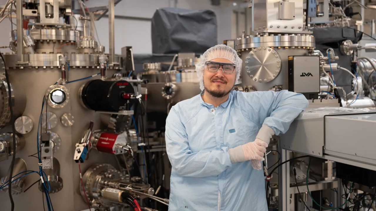
Patrick Strohbeen, a research scientist in Oliver’s Engineering Quantum Systems group, explained that the system’s ability to maintain a space-like vacuum environment around the wafers ensures high precision and reproducibility. The XPS chamber allows in situ analysis of buried interfaces, a historically challenging aspect of qubit material study, enabling scientists to better understand the quantum device platforms they develop.
MIT.nano’s Role in Supporting Quantum Research
MIT.nano, with its 45,000-square-foot cleanroom space and advanced infrastructure, was selected for housing this sensitive tool because it provides stable environmental controls and expert staff capable of managing such complex equipment. The facility’s ultra-clean environment minimizes variables like humidity and particle counts that could affect film growth and qubit yield.
Nick Menounos, associate director of infrastructure at MIT.nano, credited early collaboration and foresight with enabling an expedited installation process, reducing setup time from several months to under three weeks. Having the MBE system integrated within MIT.nano’s cleanroom also supports adjacent device fabrication and metrology tools, facilitating seamless research workflows.
Why it matters
Improving qubit performance and scalability is critical for advancing quantum computing technology. The MBE system’s capability to produce high-quality materials and characterize their interfaces in situ addresses key challenges that have limited qubit reproducibility and robustness. This development aligns with MIT’s strategic Quantum Initiative and aids national security and scientific innovation efforts by improving fundamental quantum device technologies.
Sources
This article is based on reporting and publicly available information from the following source:
Read more Science & Technology stories on Goka World News.