MIT researchers have developed a new fabrication technique called “implosion carving” that produces nanoscale photonic devices by shrinking patterned hydrogel structures to about 1/2,000 of their original volume. This method enables the creation of features smaller than 100 nanometers—smaller than the wavelength of visible light—allowing precise control of light for optical computing and other applications.
Implosion Carving Technique
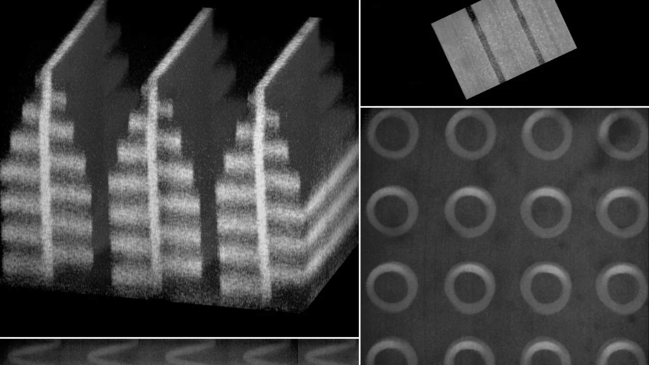
The team advanced “implosion fabrication,” originally developed at MIT in 2018, to create “implosion carving,” a process that uses lasers to generate nanoscale vacancies within a hydrogel. Researchers first coat the hydrogel with a photosensitizing dye, then employ a laser to activate the dye at specific points, generating reactive oxygen species that break chemical bonds and carve voids. These vacancies possess distinct optical properties relative to the surrounding gel.
After patterning, the hydrogel undergoes a two-step shrinking process. Soaking it in an ionic solution causes it to contract about tenfold in each dimension, followed by supercritical drying to remove liquid without damage. The resulting shrinkage reduces the volume by more than 2,000 times, shrinking 800-nanometer patterns to under 100 nanometers.
Optical Computing Demonstrations
The researchers fabricated complex 3D shapes, including helices and butterfly-wing-inspired designs, which are difficult to produce with conventional two-photon lithography due to structural instability at such thin scales. Additionally, they created a photonic device capable of performing digit classification, a computational task commonly used to assess neural networks.
This optical device diffracts input light through multiple patterned hydrogel layers, causing output light to correspond to specific digit inputs. By programming vacancy patterns throughout the device, it effectively operates as a neural network entirely using light. The research team highlighted the ability to finely control material properties at millions of points, enabling optimization through deep-learning algorithms for novel optical system designs.
Future Applications
The technique paves the way for advanced optical devices that could classify cells in flow microfluidic systems, potentially identifying rare circulating tumor cells in blood samples. It also holds promise for rapid imaging methods applicable to tissue biopsies and surgical specimen analysis. Furthermore, adapting this method for hydrophobic polymers may facilitate the creation of 3D nanofluidic channels.
Background
Conventional nanoscale fabrication approaches face limitations in resolution and three-dimensional structuring essential for manipulating visible light, which ranges from approximately 380 to 750 nanometers in wavelength. Two-photon lithography achieves feature sizes typically larger than 100 nanometers, and electron-beam lithography, while capable of finer features, is restricted to planar silicon surfaces. The implosion carving method addresses these challenges by combining precise 3D vacancy patterning with substantial volumetric shrinking to reach nanoscale resolution suitable for visible-light photonics.
The findings appear in the journal Nature Photonics and involve contributions from senior authors Peter So and Edward Boyden of MIT. Funding was provided by various foundations, including the U.S. Army Research Office, the Howard Hughes Medical Institute, and the National Institutes of Health.
Sources
This article is based on reporting and publicly available information from the following source:
Read more Science & Technology stories on Goka World News.