Scientists at MIT and the Department of Energy’s Oak Ridge National Laboratory have developed a novel technique that can move tens of thousands of atoms inside materials in three dimensions within minutes at room temperature. This breakthrough enables precise reprogramming of atomic structures deep within a material, a capability not possible with previous methods limited to two-dimensional surface rearrangements or slow processes under ultracold, high-vacuum conditions.
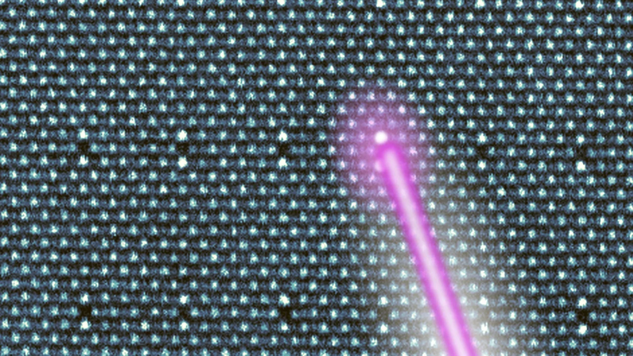
The approach uses advanced algorithms to control an electron beam that directs atomic motion by scanning specific locations inside a crystal lattice. The beam follows an oscillating path that nudges columns of atoms to new positions with picometer precision—about one trillionth of a meter. By creating atom-sized vacancies and displaced atoms in a semiconductor material known as chromium sulfide bromide, the team formed more than 40,000 quantum defects across a 13-nanometer-thick crystal within approximately 40 minutes.
MIT Research Scientist Julian Klein, who led the project, explained that the technique can “reprogram materials to create defects at will,” enabling artificial states of matter with potential applications in sensing, optics, and magnetic technologies. The team’s Nature publication highlights how engineered atomic patterns inside the material could simulate complex electronic structures akin to those in molecules.
Frances Ross, MIT’s TDK Professor of Materials Science and Engineering, noted that the ability to arrange atomic defects beneath a material’s surface creates more robust quantum systems. Unlike previous methods, which positioned atoms only on surfaces and required slow, highly controlled environments, this new process can be applied under ambient laboratory conditions and scaled to manipulate thousands or even millions of atoms.
Why it matters
This advancement addresses a longstanding limitation in materials engineering for quantum technologies, enabling the creation of stable quantum defects protected from environmental exposure. Such defects form the basis of various quantum devices, including quantum computers, atomic-scale logic devices, and dense magnetic memories. The scalability and three-dimensional control offered by this technique open new avenues for designing programmable matter with customizable quantum properties.
Background
The ability to manipulate individual atoms was first demonstrated in 1989 when IBM researchers arranged 35 atoms to spell out “IBM” on a chilled crystal surface using a scanning tunneling microscope. Since then, atomic manipulation methods have focused mainly on surface-level rearrangements or optical and ion trapping in vacuum systems. These approaches have been critical for quantum science but limited by slow operation speeds and environmental constraints.
The MIT-led team’s methodology relies on precision electron beam control combined with optimized algorithms developed over several years. This allows rapid acquisition of positional information with minimal electron exposure to avoid damaging crystals, enabling rapid, repeated atomic rearrangements within the bulk of a material, a capability essential for practical quantum device development.
Future directions
Researchers are exploring other crystalline materials where their technique might apply, anticipating broad relevance across quantum materials research. The method’s ability to build intricate atomic arrangements promises new experimental platforms for investigating collective electronic and magnetic phenomena and could accelerate innovations in materials science and quantum engineering.
The project received funding support from the U.S. Department of Energy and the National Science Foundation.
Sources
This article is based on reporting and publicly available information from the following source:
Read more Science & Technology stories on Goka World News.