Researchers at MIT have pioneered a new approach to enhance the thermal management and performance of gallium nitride (GaN) transistors, which are critical components in high-power wireless communication systems. By embedding GaN transistors into an ultrathin diamond substrate, they have achieved superior heat dissipation, allowing transistors to perform at peak levels without reliability loss.
What Happened
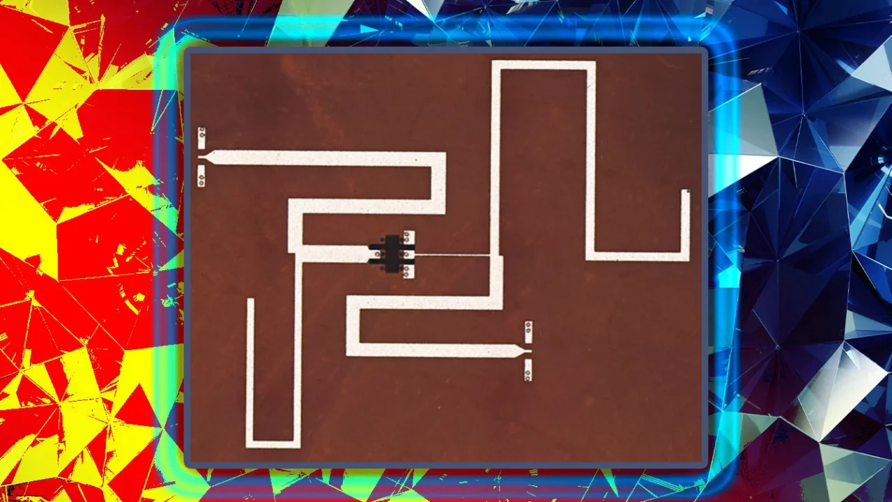
The MIT research team developed a fabrication technique that integrates tiny GaN transistors, called dielets, into single-crystal diamond layers. This diamond interposer serves as an efficient heat spreader, balancing temperatures across the transistor and underlying silicon layers. Their new power amplifier, constructed using this method, outperformed comparable devices in output power, efficiency, and gain.
Key Facts
- GaN transistors can handle higher speeds and power than silicon but generate significant heat that limits reliability and performance.
- The team used lab-grown single-crystal diamond, renowned for its exceptional thermal conductivity, as the substrate to manage heat effectively.
- The fabrication process involved femtosecond laser cutting of GaN dielets and precise placement onto diamond cavities with a thermally conductive die attach film.
- The resulting power amplifier supports longer-distance wireless transmission with improved efficiency compared to previous designs.
- The approach mitigates unwanted capacitances seen in earlier methods where diamond was grown directly on GaN, preserving transistor speed.
Why It Matters
Efficient heat dissipation in semiconductor devices is a critical challenge that constrains the speed, power, and durability of wireless communication hardware. This breakthrough offers a scalable solution for thermal management in GaN-based electronics, which are key to demanding applications such as 6G networks, satellite communications, high-power radars, and industrial drones.
Background
Traditional silicon chips cannot handle the heat and power requirements of modern wireless systems. GaN is a promising material for future electronics due to its ability to operate at high power and frequency. Previous efforts to improve thermal management involved stacking different materials, but the mismatch in thermal properties caused reliability issues.
Diamond’s unmatched thermal conductivity has been explored as a heat spreader, but earlier integration efforts introduced electrical performance issues due to parasitic capacitances.
Analysis
The MIT team’s innovation lies in embedding the GaN transistors as separate dielets into the diamond substrate rather than growing diamond over GaN. This configuration evades the capacitive drawbacks and maintains efficient heat transfer through a carefully engineered interface, including a 20-micron-thick die attach film optimized for thermal conduction.
The precision of laser-cutting and cavity alignment enables reproducibility at commercial scales, addressing both performance and manufacturing challenges.
Who Is Affected
This advancement primarily benefits industries relying on high-performance wireless communication technologies, including telecommunications, aerospace, defense, and data centers. Manufacturers of power amplifiers and high-speed electronics stand to gain from improved device reliability and efficiency.
Reactions / Official Statements
Lead author Pradyot Yadav noted this development may unlock scalability and reliability for heterogeneously integrated wireless systems, marking a significant step toward commercial adoption. Collaborators from Georgia Tech and Penn State University also contributed, highlighting interdisciplinary efforts in this progress.
What Remains Unclear
This information was not confirmed in the reviewed sources regarding long-term durability under diverse operational conditions and the exact cost implications for mass production beyond initial fabrication feasibility.
What Comes Next
The researchers aim to extend this method to more complex heterogeneous systems and anticipate that their thermal management technique will encourage the development of advanced next-generation electronics. Further work may focus on optimizing integration processes and testing scalability for commercial applications.
Sources
This article is based on reporting and publicly available information from the following source:
Read more Science & Technology stories on Goka World News.